Johns Hopkins ChemEs Crack Crucial Chip Challenge
Key Highlights
Chemical liquid deposition creates new opportunities: Johns Hopkins researchers developed chemical liquid deposition, a scalable process using familiar equipment and aqueous solutions to create amorphous zeolitic imidazolate frameworks (aZIFs), enabling manufacturers to produce semiconductor materials with existing chemical industry infrastructure.
Packing more into smaller chips: The aZIF materials work as highly sensitive positive-tone resists that can withstand high-powered radiation needed for creating microscopic circuits invisible to the naked eye.
Dual-purpose technology: Beyond semiconductor applications, aZIFs serve double duty as gas-separation membranes for chemical processing.

Researchers at Johns Hopkins University have created electronic circuits so small that they are invisible to the naked eye, solving the chip manufacturers’ headache of how to squeeze smaller features onto their products in a way that is suitable for a production line.
Currently, manufacturers coat silicon wafers with a radiation-sensitive material known as a resist. When a beam of radiation is applied to it, a chemical reaction burns details into the wafer. However, the high-powered beams needed to carve out these ever-smaller details don’t interact strongly with traditional resists.
“While the advanced lasers required for imprinting on the miniscule formats already exist, researchers needed new materials and new processes to accommodate ever smaller microchips,” explained lead researcher Michael Tsapatsis, a Bloomberg Distinguished Professor of chemical and biomolecular engineering at Johns Hopkins.
The research team had previously shown that new resists made of amorphous zeolitic imidazolate frameworks (aZIFs) could withstand the higher-powered radiation sources being tested.
Working with Swiss, Chinese and other U.S. research organizations, the group developed a new methodology called chemical liquid deposition (CLD). Using this, researchers can study various combinations of aZIFs easily and quickly, according to a Sept. 11 article in Nature Chemical Engineering.
The CLD Breakthrough
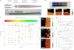
At the heart of the process is a 3D-printed reactor with a well-stirred mixing region, leading to a laminar flow coating region.
Aqueous solutions of zinc nitrate and 2-methylimidazole (2-mIm) linker are fed into the reactor separately at 2 ml/minute via a two-channel syringe pump. The two solutions merge and enter the 0.24 ml well-stirred section for vigorous mixing by a stir bar.
After a few seconds there, a moderately reactive, non-aggregated liquid mixture forms, from which smooth and continuous aZIF films can be continuously deposited by CLD under laminar flow conditions in the reactor’s second section.
The flow field in the microreactor is designed to allow the results of film depositions to be analyzed quantitatively.
To demonstrate a wider applicability of the CLD method, the researchers formed aZIF films of Zn-benzimidazole (aZIF-Zn/BIm), Zn-4,5-dichloroimidazole (aZIF-Zn/dcIm) and Co-2mIm (aZIF-Co/2mIm).
They found aZIF-Zn/BIm to be a particularly sensitive positive-tone resist. These are crucial qualities. The first means high-resolution patterning happens with lower energy than needed with traditional resists, while the second means that areas of film exposed to the electron beam become more soluble and are subsequently removed during the liquid-phase development process.
This research creates major opportunities for the chemical industry. The CLD method uses familiar equipment and aqueous solutions, making it ideal for chemical manufacturers to scale up. The aZIFs have dual applications as next-generation photoresists for semiconductor manufacturing and as gas-separation membranes for chemical processing. This positions chemical companies as essential suppliers to the semiconductor industry while also improving their own separation processes.
aZIF Evolution and Project Funding
aZIFs and their applications are the latest in a long line of technical advances made by the Tsapatsis research group. In 2009, for example, the group gave one of the first-ever demonstrations of gas separation by a metal organic framework (MOF) membrane.
In 2015, the researchers started investigating crystalline ZIFs as membranes for propane/propylene and other gas separations and three years later developed a solvent-free thin-film synthesis method based on atomic layer deposition to make them.
“At the same time, we realized that solvent-free methods also provide an avenue for aZIFs, and with support from the U.S. Department of Energy, started efforts to deposit aZIF films by molecular-layer deposition (MLD),” Tsapatsis explained.
Advanced Functional Materials published the group’s first report of aZIF film synthesis by MLD in 2024.
DOE and the National Science Foundation (NSF) are funding part of the project, and Tsapatsis said he is writing a proposal for more, so the method can be extended to other amorphous and crystalline ZIFs and MOFs.
“Although conceptually feasible, there is considerable effort required to identify deposition conditions for high-quality films when a metal and/or imidazole is substitute for another,” he said.
In May, the group won NSF funding for a $500,000, two-year project to investigate how underlying chemical reactions associated with the new process help it avoid the unwanted and indiscriminate physical sputtering effects associated with traditional plasma-based etching processes.
In September, the group received another $3.54 million from NSF to install and establish a high-tech facility to advance photoresist research in extreme ultraviolet radiation (EUV) lithography at Johns Hopkins. The facility will be available for use by scientists and engineers across the U.S. and, as well as increasing fundamental knowledge about EUV-driven chemistry, will also develop resist design principles for diverse material classes.
The next engineering challenge for the team is scaling up from 100-mm wafers used in the lab to industry standard 300-mm wafers, according to Tsapatsis.
“We will be looking for funding to start this scale up work,” he said.
Meanwhile, funding from DOE’s basic energy sciences separation program is ensuring that the membrane separation potential of the new films can be investigated, too.
Asked if any of this work had attracted industrial interest or investment, Tsapatsis replied, “Not that I can talk about.”
About the Author

Seán Ottewell
Editor-at-Large
Seán Ottewell is a freelance editor based in Ireland. He has an impressive background in the chemical industry. After earning his degree in biochemistry at Warwick University, UK, he earned his master's in radiation biochemistry from the University of London. His first job out of school was with the UK Ministry of Agriculture, Fisheries and Food, London, where he served as scientific officer with the food science radiation unit.
From there he entered the world of publishing. In 1990, he was the assistant editor of The Chemical Engineer, later moving on to the chief editor's position. Since 1998, he has been a regular contributor to European Process Engineer, European Chemical Engineer, International Oil & Gas Engineer, European Food Scientist, EuroLAB, International Power Engineer, published by Setform Limited, London, UK.
Chemical Processing has been proud to call Ottewell Editor at Large since 2007.
He and his family run a holiday cottage in the small village of Bracklagh in East Mayo. He also fancies himself an alpaca farmer.